Terraria: NOR-based SR Latch

The coolest thing to me about Terraria is that it’s not limited to just exploration and crafting, and how it also includes a full wiring and logic system.
The game provides logic gates (AND, OR, NAND, NOR, XOR, XNOR), logic gate lamps (which act as gate inputs), and signal propagation through multiple wire colors.
Because of this, Terraria is Turing complete, meaning that in theory, it can perform any computation that a universal Turing machine can.
And this is amazing because it means that you can create some crazy stuff. While most players see wiring as useful only for basic things like opening doors, teleporting, or farms, you can go much deeper.
People have built calculators, 32-bit computers, satellites, and even other games running inside Terraria. You can (in theory) literally create Terraria within Terraria. All of these allow you to observe real computational principles applied inside a 2D sandbox game.
While in theory the possibilities with Terraria’s wiring system are endless, practical limits (world size, complexity, etc.) are unfortunately reached pretty quickly.
Even so, computation in Terraria is still worth exploring. It’s a great way to visualize and understand concepts while having fun.
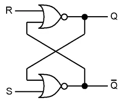
One of the simplest circuits in digital electronics is the NOR-based SR latch. It can store a single bit of information.

For my SR latch, I used:
2 switches (acting as the S and R inputs)
2 NOR gates
4 logic lamps
4 actuators
4 gemstone blocks
4 different-colored wires
I used shadow paint as my background so the circuit is easier to see. I got all my items from the Builder’s Workshop.

First, set up the switches, gates, and logic lamps like this:

Next, connect the S and R inputs to their corresponding NOR gates using different wire colors:

Now, feed the outputs of each NOR gate back into the opposite gate as inputs:

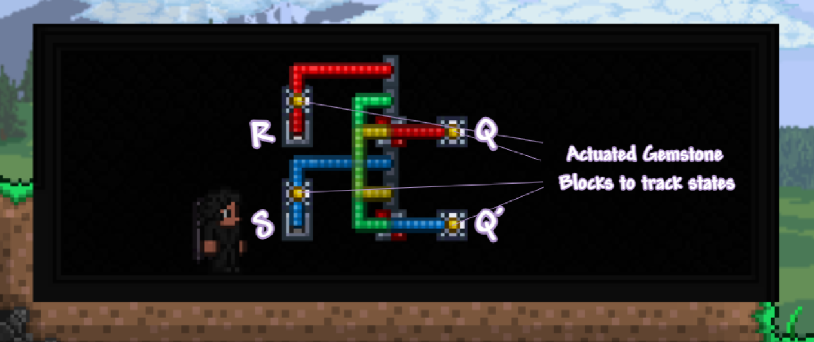
And finally, wire the outputs to actuated gemstone blocks. You can place actuated blocks along the S and R input paths to visually track their states as well:

We’re finished building, but the circuit is not ready yet. We need to do something important: synchronize the logic.
If you look at the circuit now, all logic lamps are OFF, while both Q and Q′ are ON. This is clearly incorrect. Q and Q′ must always be opposites, and NOT (0 OR 0) = 1.
A state where all logic lamps are OFF is logically impossible in this circuit.
To fix this, we must first choose an initial state. Let’s say we want Q = 1. From the truth table, we know this occurs when S = 1 and R = 0.
Temporarily unwire everything connected to the gates and logic lamps.

Using an actuation rod, manually turn Q′ OFF so that only Q remains ON. Now Q and Q′ are opposites. Next, turn the block connected to R OFF, and toggle the S switch once, so it is ON.
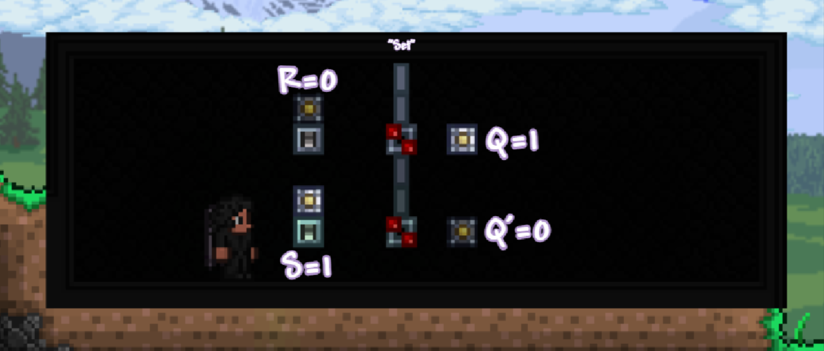

Since S = 1, the logic lamp connected to it must be ON.
Additionally, the output of the top NOR gate is:
NOT (0 OR 0) = 1
This output feeds into the bottom NOR gate, meaning both input lamps for the bottom gate must be ON.
Replace the bottom gate’s lamps accordingly:


Now, all logic states are consistent. You can now reconnect all wires.

The SR latch now works correctly and matches its truth table perfectly.
We’ve successfully stored a bit of information using a NOR-based SR latch.
What if S = R = 1? Let’s calculate:
Q = NOT (R OR Q’)
Q = NOT (1 OR Q’)
Q = NOT (1)
Q = 0
Now, Q′:
Q′ = NOT (S OR Q)
Q′ = NOT (1 OR Q)
Q′ = NOT (1)
Q′ = 0
Let’s turn S and R ON to see what happens:
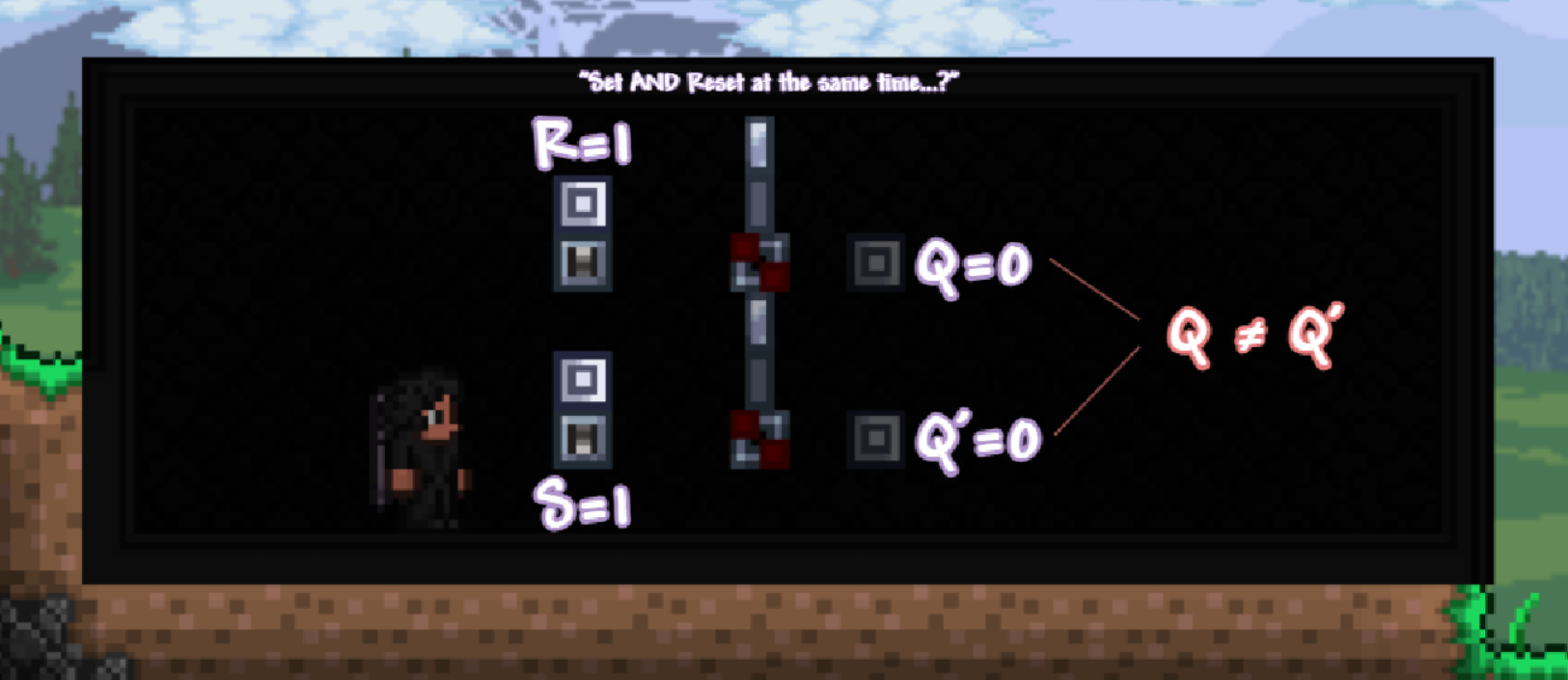

This behaviour matches our calculation.
This was just a fun experiment I decided to do while I was taking a computer architecture class.